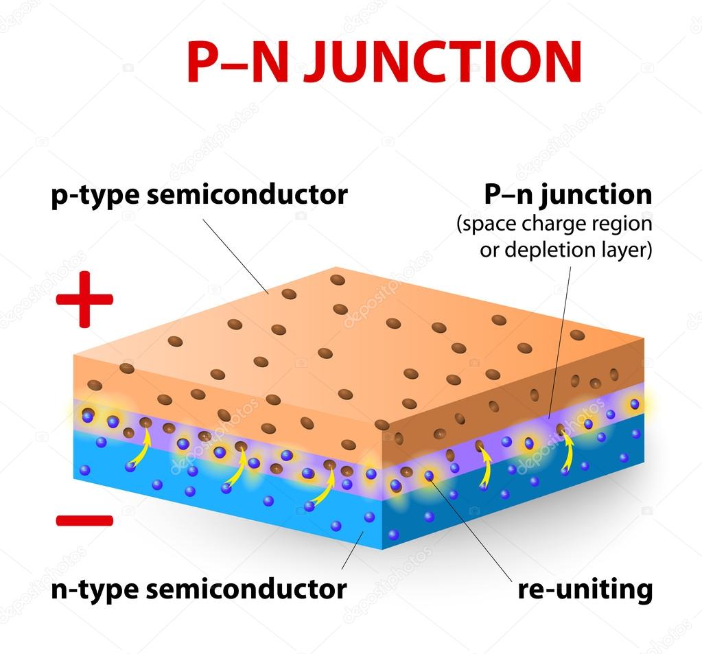
P-n junction. p-type silicon layer contains more positive charges, called holes, and the n-type silicon layer contains more negative charges, or electrons. When p-type and n-type materials are placed in contact with each other. premium vector by edesignua

Please buy a commercial licence for commercial use without attribution.
vector element illustration crystal light solar electric electrical voltage elements structure cross fingers electronics panel learning education laboratory science Materials negative section gate positive layer physics scientific type scheme silicon semiconductor led diode diagram junction ladies transistor ion p schematic n charges diffusion implantation doping contains electrons dopants epitaxy n type
Categories:Array ( ) 1
tags:
vector
element
illustration
crystal
light
solar
electric
electrical
voltage
elements
structure
cross
fingers
electronics
panel
learning
education
laboratory
science
Materials
negative
section
gate
positive
layer
physics
scientific
type
scheme
silicon
semiconductor
led
diode
diagram
junction
ladies
transistor
ion
p
schematic
n
charges
diffusion
implantation
doping
contains
electrons
dopants
epitaxy
n type